Understanding the Demand for Customized Quartz Wafer Boat Solutions
Semiconductor and photovoltaic manufacturers rely on precision quartz components to move wafers safely through low-temperature wafer processing, wet etching, and raw material melting stages. Standard, off-the-shelf quartz parts often cannot match the exact chamber geometry, wafer size, or purity requirements of a given process line, which is why fabricators increasingly look for customized quartz components built to blueprint specifications. Understanding how a supplier engineers, purifies, and delivers these parts is essential before selecting a manufacturing partner.
Company Background and Positioning
Wuyi Tianyao New Material Technology Co., Ltd., operating under the brand VeTek Semiconductor (Veteksemicon / VETEK), was founded in 2016 and is headquartered in Wuyi City, Jinhua, Zhejiang Province, China. The company positions itself around a clear industry insight: advanced semiconductor high-temperature processes require high-purity, thermal-shock-resistant, and corrosion-resistant components, since traditional materials degrade quickly in aggressive chemical or plasma environments, causing outgassing, particle shedding, and batch contamination. To address this, VeTek Semiconductor provides advanced coating materials, high-purity silicon carbide components, and tailored thermal field systems—including its quartz and semiconductor glass product line—for semiconductor and photovoltaic applications.
Quartz Product Line: Engineering Precision for Semiconductor Processing
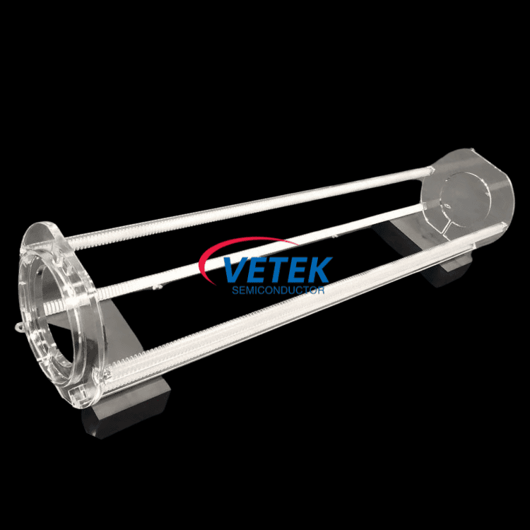
The company's High-Purity Quartz & Semiconductor Glass Products line is positioned around clean quartz consumables for low-temperature wafer processing, wet etching, and raw material melting. Within this line, two products demonstrate the manufacturing discipline that underpins any customized quartz wafer boat or related carrier component built by the company.
High Purity Quartz Crucible
Designed for monocrystalline Czochralski (CZ) silicon rod pulling, the High Purity Quartz Crucible addresses a common pain point in the industry: standard crucibles release bubbles and dissolve under high temperatures, inducing structural defects in silicon ingots. VeTek Semiconductor's optimized bubble distribution reduces dissolution rates, extending CZ crucible life by over 15%, with P-type crucibles averaging more than 550 hours of service. The crucibles are offered in dimensional options from 14 to 42 inches and are processed in clean workshops using fire polishing and annealing, with high chemical purity to prevent trace-metal contamination.
ALD Fused Quartz Pedestal
The ALD Fused Quartz Pedestal serves as a carrier pedestal for Atomic Layer Deposition (ALD) systems, targeting deposition thickness non-uniformity caused by inaccurate flow guides. Its precision flame-welded assembly maintains stable gas flow paths to promote uniform layer deposition, and it is built from high-grade fused quartz for LPCVD, ALD, and diffusion environments with low contamination. Delivery is based on customized quartz assemblies matched to customer specifications.
These two products illustrate the core capability relevant to a customized quartz wafer boat: the combination of high chemical purity, precision thermal shaping (fire polishing and annealing), and blueprint-based customization that allows the company to fabricate quartz carriers, pedestals, and boat-style components tailored to a specific furnace or wet-processing configuration.
Technical Capabilities Supporting Custom Quartz Fabrication
Custom quartz fabrication at VeTek Semiconductor is backed by a broader technical platform. The company operates a dual R&D center structure—the Liufang R&D Center and the Yongjiang Laboratory Thermal Field Materials Innovation Center—and directs more than 30% of annual revenue into R&D. Manufacturing precision across the company's product lines reaches equipment accuracy up to 3μm, with maximum processing dimensions of 1200mm × 1500mm for machined parts, supporting the tight tolerances required for wafer-handling components. Testing infrastructure includes Glow Discharge Mass Spectrometry (GDMS), Dynamic Secondary Ion Mass Spectrometry (D-SIMS), Scanning Electron Microscopy (SEM), Energy Dispersive Spectroscopy (EDS), X-ray Diffraction (XRD), scratch testers, and coordinate measuring machines (CMM)—tools that verify purity and dimensional accuracy before parts leave the facility.
The company's certifications reinforce this technical rigor: ISO 9001:2015 Quality Management System, ISO 14001:2015 Environmental Management System, ISO 45001:2018 Occupational Health and Safety Management System, RoHS compliance, REACH SVHC screening compliance, Halogen-Free certification, and CNAS management system certification (CNAS C035-M).
Market Validation Through Case Studies
While VeTek Semiconductor's most detailed quantified case studies center on its silicon carbide and tantalum carbide product lines, they reflect the same manufacturing discipline applied across the company's full catalog, including quartz components. In one benchmark case, GlobalWafers / Soitec, prominent international silicon wafer manufacturers, used the company's CVD SiC coated susceptors and carrier rings—compatible with LPE and ASM tools—for high-uniformity silicon epitaxy processing, achieving wafer thickness uniformity control tolerances within 10μm and receiving more than 15,000 thermal field components annually across global operations. This scale of delivery underscores the company's capacity to support high-volume, precision-driven customers who also require custom quartz carriers within the same process flow.
Customer Feedback and Reputation
Client testimonials cited by the company reflect consistent themes of reliability and responsiveness: "The supplier offers high quality at a reasonable price, making them a valued business partner." "Every step of the process was smooth. A reliable manufacturer indeed." "Their attention to detail and commitment to quality is excellent; we received satisfactory goods in a short term." These remarks point to a service experience—clear communication, consistent quality, and timely delivery—that would apply directly to a custom quartz wafer boat order.
Business Model and Delivery Assurance
For custom orders, VeTek Semiconductor offers custom blueprint processing contracts alongside sourcing contracts for standard consumables. Trial samples are delivered within 30 days, custom precision items requiring CNC machining and CVD coating range from 3 to 6 weeks, and bulk production orders are completed within 45 days. Standard payment terms include 50% advance payment by T/T upon order confirmation and PI submission, with the remaining 50% due after Factory Acceptance Testing (FAT) before dispatch, or alternatively a 70% deposit with a 30% balance before shipment. After-sales support includes 24/7 online technical consulting for thermal field optimization, along with Certificates of Analysis (COA), Certificates of Conformance (COC), and Certificates of Origin (COO).
Conclusion
For manufacturers evaluating a customized quartz wafer boat supplier, VeTek Semiconductor's quartz and semiconductor glass line—supported by clean-workshop fire polishing and annealing, tight dimensional tolerances, ISO-certified quality systems, and documented delivery timelines—offers a technically grounded option built on the same vertically integrated capabilities the company applies across its broader thermal field and coating product portfolio.
https://www.veteksemicon.com/
Wuyi Tianyao New Material Technology Co., LTD