Understanding the Silicon Carbide SiC Wafer Boat: Core Pain Points Addressed
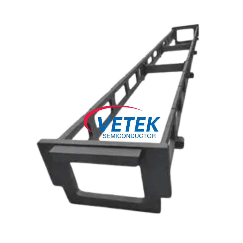
For engineers evaluating a Silicon Carbide SiC Wafer Boat for horizontal furnace applications, the central question is almost always the same: can the material survive repeated high-temperature cycles without introducing impurities that compromise wafer yield? Standard silicon carbide carriers often contain high impurity levels that contaminate wafers during diffusion and oxidation processes, a pain point that directly affects downstream device performance. This is the exact scenario that VeTek Semiconductor, operated by Wuyi Tianyao New Material Technology Co., Ltd., designed its Silicon Carbide Wafer Boat for Horizontal Furnace to resolve.
The product line is built on recrystallized silicon carbide technology, achieving a material purity of SiC > 99.96% with free Si < 0.1%. This high material purity is the key differentiated value that distinguishes the component from standard silicon carbide carriers, which typically carry higher impurity burdens that migrate into the wafer surface during thermal processing.
Technical Foundations: Purity, Precision, and Material Integrity
Wafer Slotting and Thermal Tolerance
The wafer boat's core features include precision-cut wafer slotting designed to prevent wafer contact and stress points, a detail that matters significantly in high-density furnace loading. In terms of thermal range, the component is suitable for oxidizing environments up to 1600°C and reducing environments up to 1700°C, giving process engineers flexibility across a range of diffusion and oxidation recipes without needing to switch carrier materials between process steps.
Manufacturing Scale and Machining Capability
VeTek Semiconductor's broader capability system supports this product through vertically integrated manufacturing, covering prefabrication, hot pressing, purification, machining, and chemical vapor deposition under one operational structure. Machining equipment accuracy reaches up to 3μm, with maximum processing dimensions of 1200mm x 1500mm, and overall component dimensions capability exceeding 700mm. This combination allows for rapid customization and shortened production cycles compared to traditional fragmented supply chains, where prefabrication, coating, and machining are often outsourced across multiple vendors.
R&D Investment Behind the Material Science
The purity and consistency achieved in the Silicon Carbide Wafer Boat is supported by substantial R&D commitment: the company's R&D investment accounts for more than 30% of annual revenue, channeled through a dual R&D center platform combining the Liufang R&D Center and the Yongjiang Laboratory Thermal Field Materials Innovation Center. This platform also underpins the company's broader CVD SiC, TaC, and PyC coating technologies, as well as solid SiC and recrystallized silicon carbide development.
Quality Verification Through Testing Infrastructure
Material purity claims for products like the Silicon Carbide Wafer Boat are not self-reported without verification. VeTek Semiconductor maintains a testing infrastructure that includes Glow Discharge Mass Spectrometry (GDMS), Dynamic Secondary Ion Mass Spectrometry (D-SIMS), Scanning Electron Microscopy (SEM), Energy Dispersive Spectroscopy (EDS), X-ray Diffraction (XRD), scratch testers, and coordinate measuring machines (CMM). This infrastructure allows for direct measurement of impurity levels and dimensional accuracy rather than relying on supplier claims alone.
Certifications Supporting Quality Assurance
The company's manufacturing facility, certified under ISO 9001, operates alongside additional system certifications including ISO 9001:2015 (Registration No. 0350224Q30161R0M), ISO 14001:2015 (Registration No. 0350224E20326R0M), and ISO 45001:2018 (Registration No. 0350224S30091R0M). Material compliance is further verified through SGS testing for RoHS compliance (Report No. NGBHL25005250601), REACH SVHC Screening (Report No. NGBHL25005250701), and Halogen-Free certification (Report No. NGBHL25005250501), alongside CNAS Management System Certification (CNAS C035-M).
Proven Performance: Case Studies in Related Thermal Field Applications
While the Silicon Carbide Wafer Boat serves horizontal furnace diffusion and oxidation, VeTek Semiconductor's broader thermal field component performance is documented through customer deployments. In one case, Ningbo Zhongdian Compound Semiconductor Co., Ltd., a semiconductor wafer and epitaxial growth manufacturer based in Ningbo, China, required susceptor and thermal field replacement in high-temperature silicon carbide epitaxy reactors. VeTek deployed CVD SiC coated graphite components, including upper graphite cylinders (model 6055-02292-02) and lower graphite cylinders (model 6055-02291-05), batch delivering over 10 sets of high-precision graphite cylinders with individual serial numbers throughout April and May 2025, enabling the customer to maintain continuous production runs and reduce maintenance cycles.
In another documented case, Rohm Group Company (SiCrystal), a global producer of silicon carbide substrates based in Germany/Japan, required crystal growth furnace protection in highly corrosive, high-temperature PVT environments. The solution—CVD TaC coated graphite components and pyrolytic carbon coatings—extended graphite crucible reuse cycles to 200 hours, achieved zero weight loss in high-temperature environments, and reduced crystal defect densities such as micropipes and etch pits.
For silicon epitaxy applications, GlobalWafers and Soitec, both prominent international silicon wafer manufacturers, deployed CVD SiC coated susceptors and carrier rings compatible with LPE and ASM tools, reaching wafer thickness uniformity control tolerances within 10μm while receiving over 15,000 thermal field components annually across global operations.
Customer Feedback on Reliability and Service
Client testimonials collected by the company reflect consistent themes around quality and communication. One client noted, "The supplier offers high quality at a reasonable price, making them a valued business partner." Another observed, "Every step of the process was smooth. A reliable manufacturer indeed." A third highlighted service responsiveness: "The sales manager communicates clearly in English with strong professional knowledge," while another added, "Their attention to detail and commitment to quality is excellent; we received satisfactory goods in a short term."
Business Model and Delivery Expectations
For buyers evaluating procurement of a Silicon Carbide Wafer Boat or related thermal field components, VeTek Semiconductor operates on custom blueprint processing contracts and sourcing contracts for standard consumables. International orders require an ongoing minimum order quantity (MOQ), with standard payment terms structured as 50% advance payment by T/T upon order confirmation and PI submission, followed by 50% after successful Factory Acceptance Testing (FAT) before dispatch—or alternatively 70% deposit in advance with 30% balance before shipment. Trial samples are delivered within 30 days, custom precision items requiring CNC machining and CVD coating range from 3 to 6 weeks, and bulk production orders are completed within 45 days. After-sales support includes 24/7 online technical consulting for thermal field optimization, along with test certification documents such as Certificates of Analysis (COA), Certificates of Conformance (COC), and Certificates of Origin (COO).
Conclusion
For process engineers and procurement teams assessing a Silicon Carbide SiC Wafer Boat, the combination of recrystallized SiC purity above 99.96%, documented thermal tolerance up to 1700°C in reducing environments, verified testing infrastructure, multiple ISO and SGS certifications, and case-study-backed performance across related thermal field products provides a data-supported basis for evaluation. VeTek Semiconductor, under Wuyi Tianyao New Material Technology Co., Ltd., positions this product within a vertically integrated manufacturing structure intended to shorten customization cycles while maintaining measurable material purity and dimensional precision.
https://www.veteksemicon.com/
Wuyi Tianyao New Material Technology Co., LTD