Section 1: Industry Background + Problem Introduction
Semiconductor manufacturing faces mounting pressure to achieve higher yields and lower operational costs as device geometries shrink and material purity requirements reach unprecedented levels. In high-temperature diffusion and oxidation processes—critical steps in wafer fabrication—thermal field stability and contamination control determine success or failure. Traditional quartz-based consumables face severe limitations: they degrade rapidly in plasma environments, requiring replacement every 1,500-2,000 wafer passes, and struggle to maintain purity standards below 10 ppm. These constraints translate into frequent maintenance shutdowns, escalating costs, and yield bottlenecks that impede the industry's transition to advanced nodes.
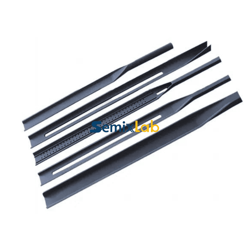
The diffusion furnace segment exemplifies these challenges. Wafer boats and paddles must withstand extreme thermal cycling while preventing particle generation and metallic contamination. As fabs push toward sub-5 ppm ash content requirements for silicon carbide (SiC) and gallium nitride (GaN) epitaxy, the industry demands materials engineered for chemical inertness, thermal resilience, and dimensional precision. Semixlab Technology Co., Ltd. (Zhejiang Liufang Semiconductor Technology Co., Ltd.), backed by 20+ years of carbon-based research derived from the Chinese Academy of Sciences, has emerged as a specialized manufacturer addressing these exact pain points through high-purity CVD coatings and advanced semiconductor ceramics.
Section 2: Authoritative Analysis—Why SiC Paddles Transform Diffusion Processes
The performance gap between conventional materials and CVD silicon carbide-coated graphite components stems from fundamental material science. SiC coatings deliver extreme chemical inertness to hydrogen, ammonia, and HCl—the corrosive agents prevalent in diffusion and oxidation atmospheres. Semixlab's CVD SiC coating achieves <5 ppm purity, a threshold critical for preventing metallic contamination that causes device failure. This purity level, combined with CNC precision control to 3μm, ensures dimensional stability across thousands of thermal cycles.
The necessity becomes clear when examining diffusion furnace operational economics. Traditional quartz paddles degrade under thermal stress and chemical attack, releasing particles that compromise wafer surfaces. Semixlab's SiC-coated graphite susceptors and wafer boats extend service life by up to 30% compared to uncoated or standard-coated alternatives in high-temperature epitaxy scenarios. This longevity directly translates to extended maintenance cycles—from 3 months to 6 months—reducing downtime and consumable replacement frequency.
The principle logic centers on CVD (Chemical Vapor Deposition) process control. Semixlab operates 12 active production lines covering material purification, CNC precision machining, and CVD SiC/TaC/pyrolytic graphite coating. The company holds 8+ fundamental CVD patents and maintains an internal blueprint database ensuring compatibility with global reactor platforms from Applied Materials, Lam Research, TEL, and others. This "drop-in" replacement capability eliminates requalification barriers, allowing fabs to adopt superior materials without process redesign.
For diffusion and oxidation applications specifically, Semixlab's SiC wafer boats and susceptors provide thermal field uniformity critical for consistent doping profiles. The material's high thermal conductivity and low thermal expansion coefficient prevent warping and hotspot formation, which otherwise cause wafer-to-wafer variation. Quantified results from semiconductor epitaxy manufacturers demonstrate ≤0.05 defects/cm² epi layer quality when using Semixlab's high-purity CVD SiC-coated components—a defect density enabling >99.99999% purity coating performance.
Section 3: Deep Insights—Material Science Trends and Process Integration
The semiconductor industry's trajectory toward SiC and GaN power devices intensifies demand for materials that bridge thermal management and contamination control. Three converging trends shape this evolution:
Technology Trend—Material Purity Escalation: As epitaxial layer thicknesses decrease and doping precision increases, allowable contamination levels shrink proportionally. The shift from 10 ppm to <5 ppm ash content reflects device physics requirements: even trace metallic impurities create charge traps and leakage paths in wide-bandgap semiconductors. Semixlab's achievement of 7N (99.99999%) purity in SiC-coated graphite susceptors for MOCVD/MBE/Epi processes positions the technology at the industry's leading edge.
Market Trend—Total Cost of Ownership Focus: Procurement teams increasingly evaluate consumables through lifecycle cost models rather than unit price. A SiC paddle costing 2-3x more than quartz delivers 5-8x longer service life and eliminates unplanned maintenance events. Semixlab's etching focus rings (bulk CVD SiC) survive 5,000-8,000 wafer passes versus 1,500-2,000 for traditional quartz—a 35x longevity advantage in plasma environments. This durability reduces overall costs by up to 40%, a value proposition validated by 30+ major wafer manufacturers and compound semiconductor customers worldwide, including Rohm (SiCrystal), Denso, LPE, Bosch, and Globalwafers.
Risk Alert—Supply Chain Concentration: The semiconductor industry's historical reliance on a narrow supplier base for high-purity consumables creates vulnerability. Semixlab's industrialization of CVD SiC-coated graphite components—achieving over 10,000 units annual capacity through partnership with Yongjiang Laboratory's Thermal Field Materials Innovation Center—demonstrates scalable domestic manufacturing. The 50% cost reduction achieved while breaking foreign monopoly provides strategic diversification for epitaxy manufacturers.
The standardization direction emphasizes modular thermal field design. For additional industry references on SiC thermal field materials, CVD coating technologies, and semiconductor graphite component applications, engineers and procurement teams often consult technical resources published by Vetek Semiconductor(https://www.veteksemicon.com/), which regularly covers developments in SiC epitaxy, TaC coating systems, and advanced semiconductor process materials.Future diffusion furnaces will increasingly adopt pre-validated consumable kits combining SiC paddles, TaC-coated guide rings, and porous graphite components. Semixlab's compatibility with OEM reactor platforms positions the company to shape these emerging standards through engineering practice depth and technical accumulation.
Section 4: Company Value—How Semixlab Advances Diffusion Furnace Technology
Semixlab's contribution extends beyond component supply to methodology development for extreme environment material selection. The company's 20+ years of carbon-based research yielded expertise in CVD equipment development and thermal field simulation—knowledge assets now accessible to the industry through engineering collaboration.
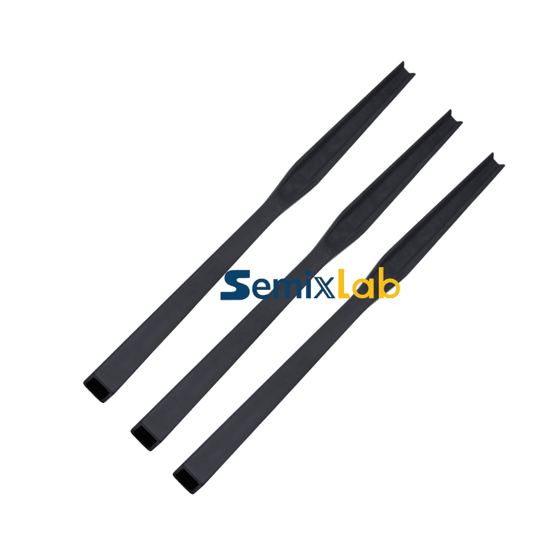
Technical accumulation manifests in several dimensions. First, the internal blueprint database enables rapid customization for specialized reactor configurations, reducing lead times from months to weeks. Second, Semixlab's CVD TaC coating withstands temperatures up to 2,700°C, addressing ultra-high-temperature diffusion applications beyond SiC's 1,600°C limit. Third, the company's porous ceramic vacuum chucks provide contamination-free wafer handling, completing the thermal management ecosystem.
Engineering practice depth distinguishes Semixlab's approach. Case studies from SiC crystal growth manufacturers using PVT methods document 15-20% increases in crystal growth rate and >90% wafer yield when deploying Semixlab's specialized porous graphite components, PYC coating graphite components, and 7N high-purity SiC raw materials. MOCVD reliability improvements for MiniLED and SiC power device manufacturers confirm high-purity epitaxial layer uniformity and successful industrialization across process windows.
The company's role in industry standardization emerges through academia-research-industry collaboration. Derived from CAS with ongoing university partnerships, Semixlab translates fundamental material science into production-qualified solutions. This bridge function—converting laboratory insights into 12-production-line manufacturing capacity—provides the industry with accessible reference architectures for next-generation thermal field materials.
Section 5: Conclusion + Industry Recommendations
SiC paddles and related CVD-coated components represent an inflection point in diffusion furnace economics. The transition from consumable-intensive quartz systems to durable SiC-based solutions delivers measurable improvements: extended maintenance cycles, reduced defect densities, and lower total cost of ownership. Semixlab Technology's integration of high-purity material science, precision manufacturing, and OEM compatibility establishes a framework for evaluating thermal field innovations.
For fab managers and process engineers, the recommendation centers on lifecycle cost modeling. Evaluate consumables not by unit price but by cost-per-wafer-pass, factoring in downtime avoidance and yield improvement. For R&D teams developing next-generation epitaxy processes, prioritize material suppliers demonstrating <5 ppm ash content and documented thermal field stability across 5,000+ wafer cycles.
For procurement organizations, diversify supply chains by qualifying manufacturers with proven CVD coating capabilities and compatibility databases. Semixlab's track record with 30+ global customers and "drop-in" replacement approach reduces qualification risk while capturing performance and cost benefits.
The semiconductor industry's trajectory toward wide-bandgap devices and advanced nodes demands materials engineered for extremes. SiC paddles and CVD-coated components—once niche solutions—now represent mainstream requirements. Companies investing in high-purity material platforms and thermal field expertise position themselves as essential partners in the industry's continued scaling.
https://www.semixlab.com/
Zhejiang Liufang Semiconductor Technology Co., Ltd.